
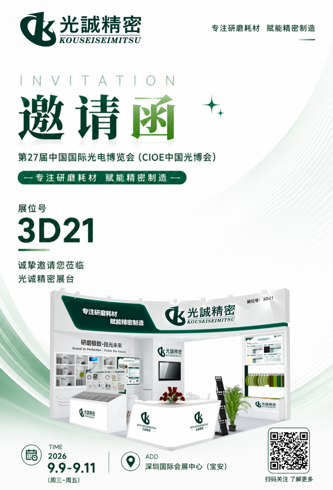
Gather with Light · Embark on a New Journey|KST Precision invites you to meet at CIOE
Focus on Precision‑Material Processing
Bosi‑KST Presents Six Industry‑Leading Solutions at CIOE 2026
Precision processing is evolving from “stand‑alone product optimization” toward “end‑to‑end process collaboration”.
Differences in material hardness, brittleness, crystal orientation, thickness and structure demand coordinated design for grinding approaches, polishing interfaces, polishing media, equipment parameters and inspection methods. Simply replacing one consumable rarely resolves efficiency, figure accuracy, surface quality and subsurface damage simultaneously.
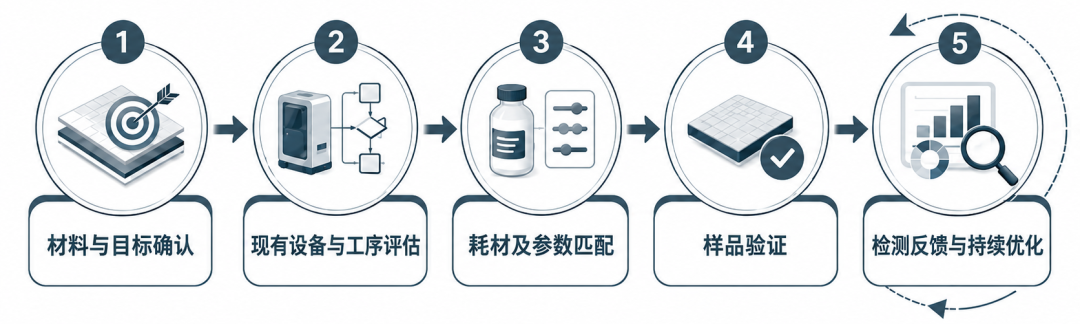
At this CIOE, Bosi‑KST demonstrates holistic solutions covering equipment evaluation, pre‑process thinning, precision polishing and metrology validation for six typical application scenarios.
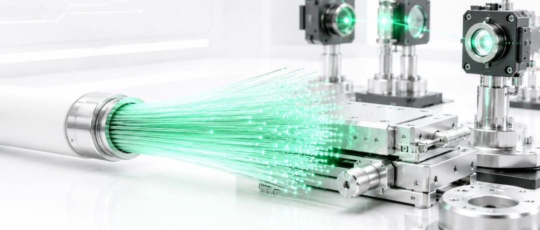
01 Co‑ordinated End‑face Processing & Inspection for MPO Optical‑communication Connectors
MPO connectors feature multi‑fiber array structures. End‑face scratches, chipping, contamination and fiber height consistency directly determine coupling performance. Our solution spans lapping, polishing, cleaning and inspection, with emphasis on end‑face geometry and batch‑to‑batch stability.
Bosi‑KST showcases tailored lapping‑and‑polishing solutions for MPO, including specially‑developed ceria abrasives and damping cloths for fiber processing.
02 Low‑stress Thinning & Synchronized Fine Polishing for InP Substrates & Chips
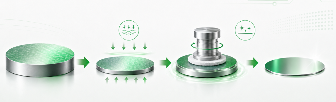
Indium Phosphide (InP) is brittle and highly susceptible to edge chipping, mechanical stress and polishing scratches. Thinning, grinding, coarse polishing and fine polishing must be performed in graduated steps to control thickness, flatness and damaged layers and prevent pre‑existing defects from propagating to final surfaces.
Bosi‑KST supplies alumina slurries (comparable to L‑141) and dual‑component silica slurries (comparable to F‑i series) for InP substrates as well as EML/VSCAL chips, together with exclusive Toray polishing pads engineered for harsh InP processing conditions.
03 SiC Substrates & Devices: Balanced Throughput and Minimal Damage
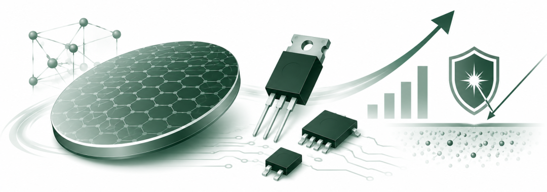
Silicon Carbide (SiC) exhibits high hardness and superior chemical stability. Our solution interconnects coarse grinding, fine grinding and chemical‑mechanical polishing to manage TTV, warpage, edge chipping, surface scratches and subsurface damage, minimizing over‑polishing allowances for downstream steps.
Bosi‑KST delivers a full‑process portfolio for SiC including grinding wheels, diamond lapping slurries, alumina slurries, silica slurries, polyurethane pads, non‑woven pads and damping cloths.
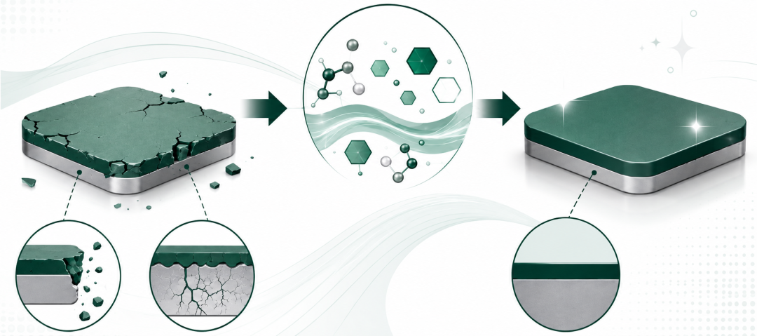
04 Chalcogenide & Precision Glass: Chipping and Sub‑surface Crack Control
Hard‑brittle glasses tend to generate edge chipping, scratches and subsurface cracks during grinding. By progressive abrasive sizing, low‑load grinding and sequential fine polishing, our solution preserves figure accuracy while removing process‑induced damage layer‑by‑layer.
Bosi‑KST has formulated proprietary alumina slurries optimized for chalcogenide glass. Compared with mainstream commercial alumina slurries, they deliver superior surface finishes with reduced scratch risk as a drop‑in alternative to imported U‑brand alumina products. Complementary diamond slurries of various grit grades are available for special operating conditions, proven in volume‑production by existing customers.
05 Process Adaptation for LT, LN and Germanium Wafers
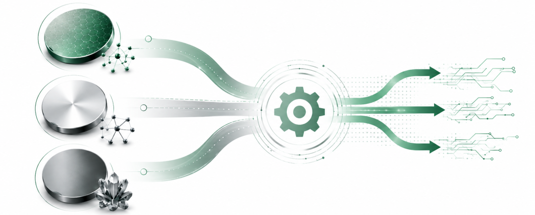
Lithium Tantalate (LT), Lithium Niobate (LN) and germanium wafers differ markedly in crystal properties and machining responses. Thinning recipes, polishing pads, slurries and cleaning protocols must be individually matched according to crystal orientation, wafer diameter, thickness and surface requirements, prioritizing thickness uniformity, warpage and surface‑defect mitigation.
Beyond standard lapping‑polishing kits for LT/LN, Bosi‑KST introduces thinning grinding wheels for germanium and custom‑formulated slurries for thin‑film LN, accelerating advances in novel optical materials.
06 Closed‑loop TGV Glass‑substrate Processing with Stress Inspection
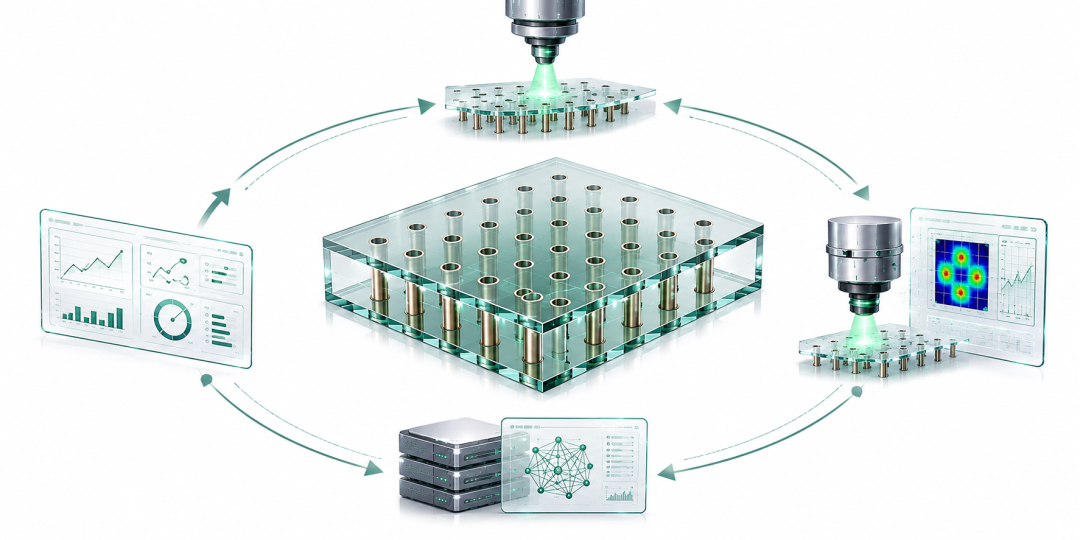
Dense through‑glass vias render TGV substrates prone to localized stress concentration and warpage during thinning and polishing. Our workflow integrates glass lapping‑polishing with PA‑micro / PA‑300L birefringence stress metrology. Stress‑distribution visualization supports process tuning and quality judgement.
Addressing common TGV customer pain‑points: low lapping throughput, long polishing cycles and high material costs, Bosi‑KST has developed novel‑abrasive lapping slurries and high‑selectivity polishing slurries to support domestic TGV process development.
 Embed Solutions into Every Process Step
Equipment delivers machining and metrology capabilities; grinding wheels perform coarse/fine grinding and dimensional control; polishing pads establish stable polishing interfaces; polishing slurries execute controlled material removal tuned to material and process stage.
The four categories — Equipment → Grinding Wheels → Polishing Pads → Polishing Slurries — work synergistically. Solution validity is ultimately judged against material properties, factory constraints and target performance metrics.
Solution Support & Contacts
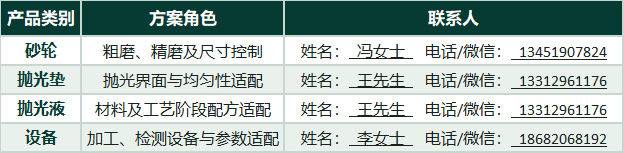
Bring your real‑world challenges for on‑site technical discussions
Booth 3D21, Hall 3‑D
Please bring samples, equipment specifications and existing process parameters.
Our KST‑Precision team will co‑engineer optimized solutions with you.
Shenzhen, September 9‑11. See you there!


