
SiC Wafers Enter the 12-Inch Era: Beyond Power Semiconductors, These New Applications Emerge!
Silicon carbide (SiC) wafers used in power semiconductors and other applications are entering the 12-inch (300mm) era. At Tokyo Big Sight's "40th NEPCON Japan" (January 21-23, 2026), multiple Chinese manufacturers exhibited 12-inch SiC wafers through Japanese distributors.
01 JSG Debuts N-Type / Optical SiC, High Thermal Conductivity Expands AI Applications
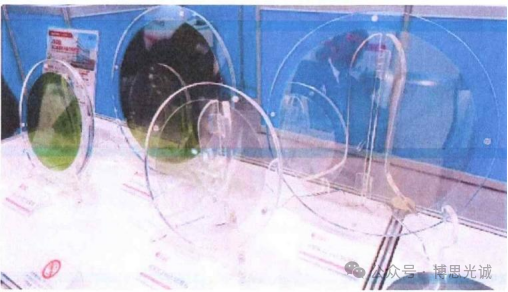
Figure 1: JSG 12-inch SiC wafers exhibited at the Maruem Shokai booth (rear left and right). Rear left is N-type, right is optical grade.
JSG displayed two types of SiC wafers: one with a thin green tint, primarily used for electronic conduction—the "N-type"; and a transparent "optical" 12-inch wafer. The distributor Maruem Shokai (Nagoya City) stated that "each wafer currently sells for several million yen." In addition to power semiconductors, N-type SiC may also be used in fields such as AI semiconductor heat-dissipation substrates that leverage its high thermal conductivity.
The thermal conductivity of SiC varies by crystal structure and purity, with high-end products reaching 400-500W/(m·K), far exceeding sapphire substrates and ranking first among ceramic materials (Figure 2). Its thermal conductivity approaches or even exceeds that of silver (Ag), the metal with the highest thermal conductivity.
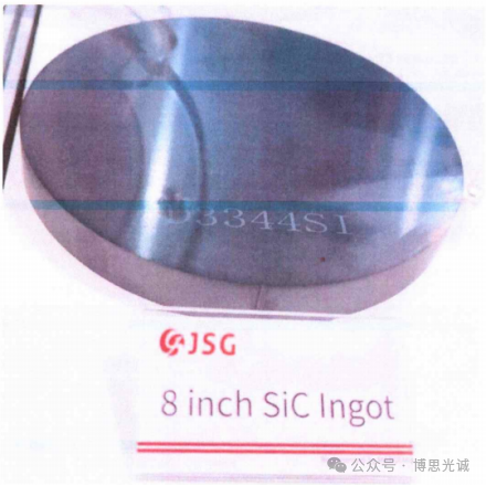
Figure 2: A JSG 8-inch silicon carbide ingot exhibited at the Maruem Shokai booth. It is sliced and lapped into wafers.
02 Semi-Insulating SiC Expands Applications; 12-Inch Wafer Companies Make Their Debut
So Do AR Glasses' Light Guides and Intermediate Spacers
Meanwhile, uncoated semi-insulating transparent optical materials are also envisioned for uses such as AR (augmented reality) glasses' light guides and AI semiconductor interposers (intermediate substrates). The high thermal conductivity of these materials has also become a key characteristic.
Maruem Shokai stated that "when shipping to Japanese SiC semiconductor manufacturers, we use epitaxial wafer form, in which a higher-quality SiC thin film is formed on the SiC wafer." It is understood that the production of epitaxial wafers is handled by Guangdong TY Semiconductor, but 12-inch SiC wafers have not yet entered mass production.
Another company exhibiting 12-inch SiC wafers is Shanxi Shuoke Crystal (SEMISiC). In January 2025, the company announced that it had become the world's first manufacturer to produce 12-inch high-purity monocrystalline SiC wafers (Figure 3).
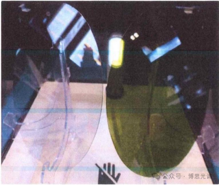
Figure 3: SEMISiC 12-inch SiC wafers exhibited at the Nishinippon Trading booth. Semi-insulating (left) and N-type (right).
Two Types of SiC Wafers Exhibited; Nishinippon Trading Showcases Multiple Wafer Types
Shanxi Shuoke Crystal also displayed both N-type and transparent semi-insulating products. The distributor Nishinippon Trading (Chuo, Tokyo) stated: "N-type has almost no shipping cases yet, but semi-insulating has already achieved small-batch shipments of up to 1,000 wafers." Notably, in addition to SiC wafers, Nishinippon Trading also exhibited diamond wafers and aluminum nitride (AlN) wafers (Figures 4 and 5).
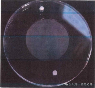
Figure 4: A diamond wafer from China's Compound Semiconductor (Xiamen) Technology Co. exhibited at the Nishinippon Trading booth. Its thermal conductivity as high as 1,000 to 2,200 W/(m·K) is a notable feature. Polycrystalline can be produced at 4 inches, monocrystalline at 1 inch.
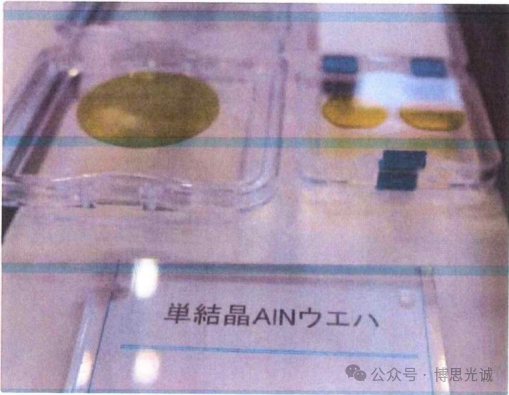
Figure 5: An aluminum nitride (AlN) wafer from China's Ultratrend Technologies exhibited at the Nishinippon Trading booth. It is said to be producible up to 3 inches.
03 SICC Pushes 12-Inch SiC and Aligns with Toshiba, Accelerating Global Expansion
The Toshiba Group and SICC Have Reached a Cooperation Agreement
In addition to the exhibitors this time, China's Shandong SICC has already announced in 2024 that it was the world's first company to bring 12-inch silicon carbide (SiC) wafers to the market. The company plans to launch a complete product line covering N-type, semi-insulating, and P-type (mainly hole-conducting) wafers in 2025. In August 2025, the company reached a preliminary agreement with Toshiba Devices & Storage on technical collaboration and business cooperation.
Related Articles
Toshiba Joins Forces with China's SICC for SiC Wafer Cooperation: Toshiba Semiconductor subsidiary Toshiba Devices & Storage announced on August 22, 2025 that it would establish a cooperative relationship with Shandong SICC, China's leading SiC (silicon carbide) wafer company.
The two parties will collaborate on the technology development and procurement of SiC wafers, aiming to provide high-quality...
Global Race for 12-Inch SiC: Multiple Chinese Companies in R&D, US Companies Launch New Platforms
In China, it has been reported that in addition to the aforementioned companies, around 7 manufacturers are developing 12-inch silicon carbide wafers.
On December 3, 2025, the US company Coherent announced the launch of a 300mm silicon carbide platform, meaning that major silicon carbide wafer manufacturers have clearly made public their development plans for 12-inch silicon carbide wafers.
END
12-Inch SiC Wafers Open a New Chapter in the Global Race
At Tokyo's NEPCON Japan exhibition, Chinese companies such as Zhejiang Jing Sheng Ji Dian and Shanxi Shuoke Crystal showcased 12-inch SiC wafers including N-type and semi-insulating types. Their high thermal conductivity also opened up new applications such as AI heat dissipation and AR light guides.
The global track is equally intense: Shandong SICC was the first to launch products and partnered with Toshiba, US company Coherent launched a 300mm platform, and another 7 Chinese manufacturers are following up with R&D. The mass production and application breakthroughs of 12-inch SiC wafers are injecting new vitality into semiconductors and downstream fields.


