
3 Solutions Field-Tested! Kousei Seimitsu Cracks the Ceramic Substrate Polishing Challenge This Way
Ceramic substrates are core components in fields such as power semiconductors and new energy vehicles. Their polishing quality directly affects product performance and lifespan. Kousei Seimitsu has launched 3 professional solutions tailored to the polishing needs of ceramic substrates. Verified through field testing and covering different requirements, they provide the industry with efficient and reliable technical support.
01 Ceramic Substrate: The "Special Circuit Board" of the Electronics Field
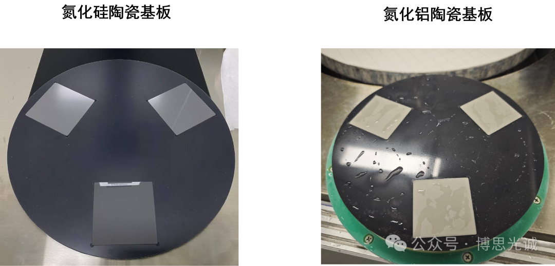
A ceramic substrate is a special process board in which copper foil is directly bonded to the surface of a ceramic substrate. Compared with conventional PCB boards, it is the "special forces" that solves the "heat" and "power" challenges.
Core Advantages
Excellent electrical insulation, high thermal conductivity, superior soft soldering performance, and high adhesion strength.
Main Classifications
Aluminum nitride ceramic substrates, silicon nitride ceramic substrates, silicon carbide ceramic substrates, beryllium oxide ceramic substrates, aluminum oxide ceramic substrates.
Application Scenarios
Extreme environments such as precision ceramics, precision optics, power semiconductors, electric vehicles, robots, and medical equipment.
02 Three Solutions Field-Tested: Let Data Speak to Precisely Match Needs
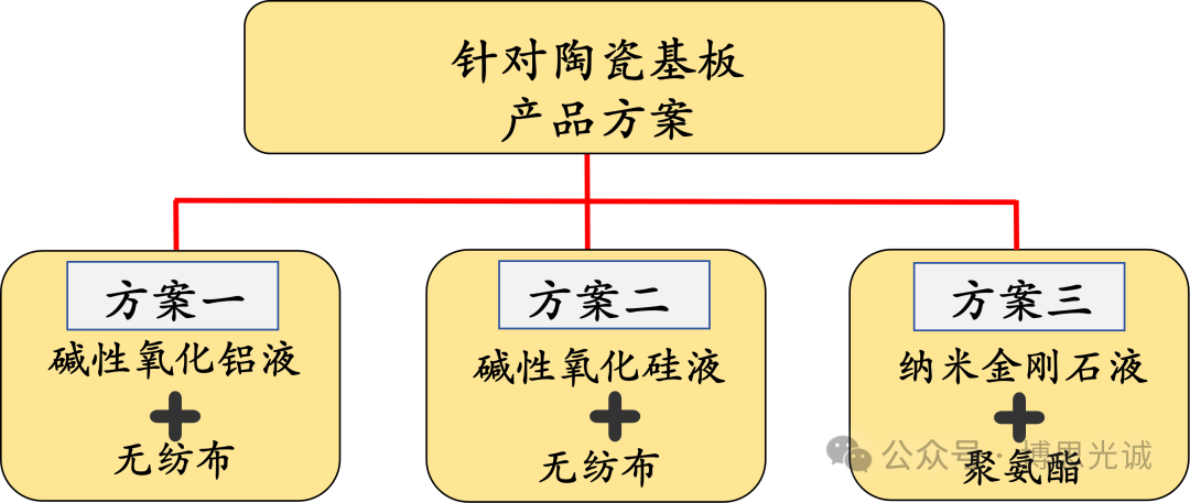
Kousei Seimitsu designed 3 differentiated solutions for polishing aluminum nitride ceramic substrates. Through standardized testing, the core performance indicators of each solution were obtained, and they can be selected as needed.
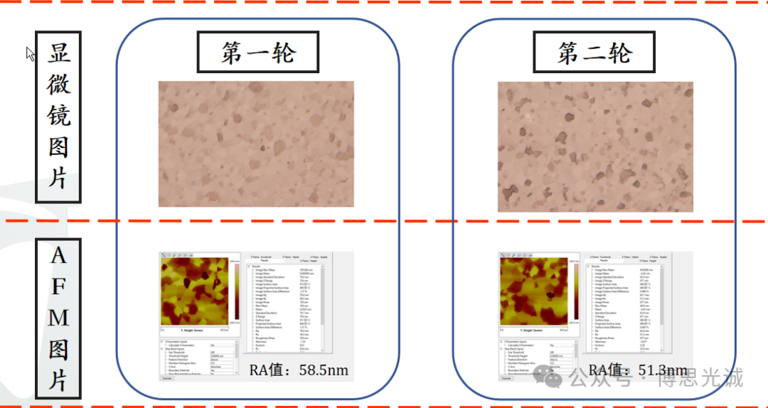
Solution 1: Alkaline Alumina Slurry + Non-Woven Fabric, Focused on High-Efficiency Removal
1. Test conditions: Equipment SPEEDFAM CT, duration 60min, speed 50rpm, load 300g/cm².
2. Core data: Overall removal rate 10-12um/h, overall RA value 50-60nm.
3. Solution advantages: The highest removal rate among the three solutions, suitable for scenarios pursuing processing efficiency.
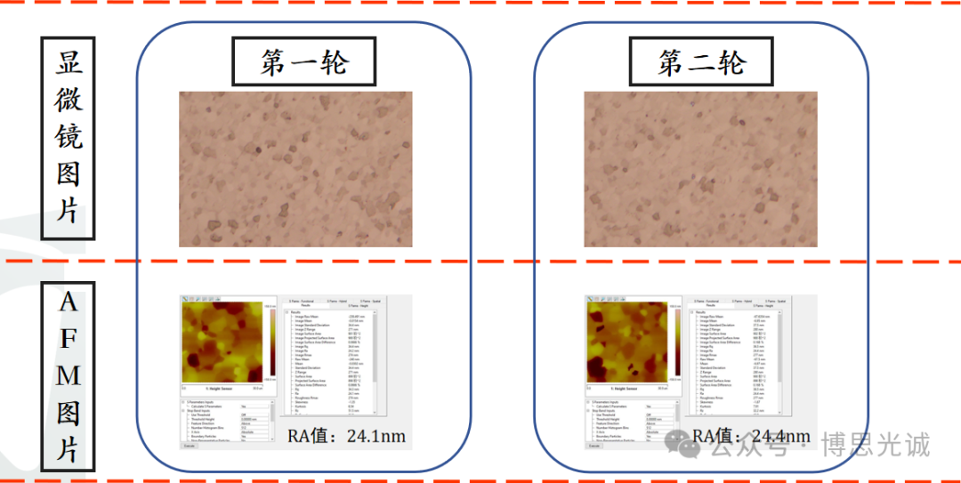
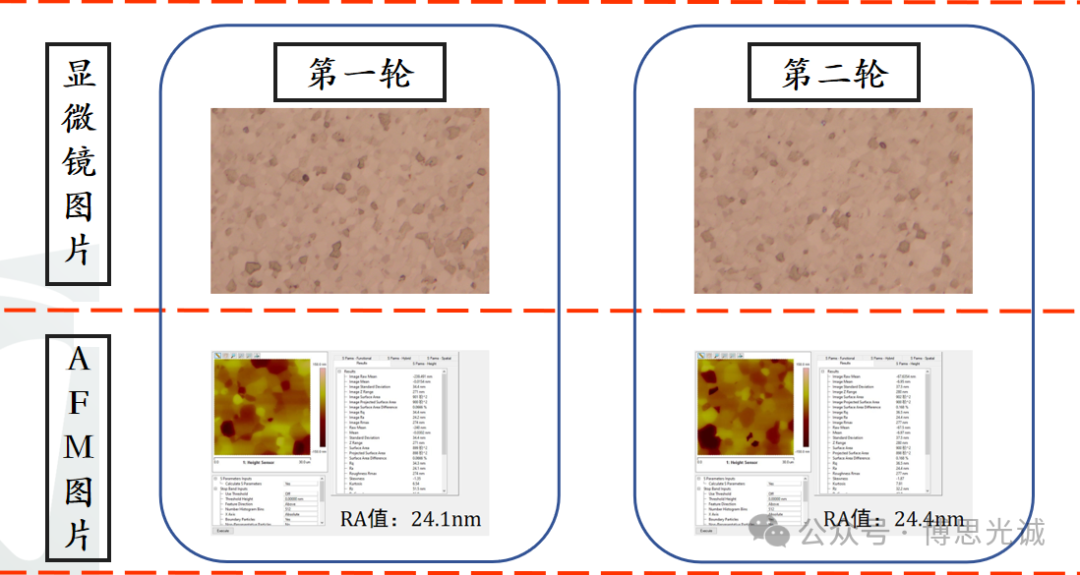
Solution 2: Alkaline Silica Slurry + Non-Woven Fabric, Focused on Low Surface Roughness
1. Test conditions: Equipment SPEEDFAM CT, duration 60min, speed 50rpm, load 300g/cm².
2. Core data: Overall removal rate 5-6um/h, overall RA value 20-25nm.
3. Solution advantages: Excellent surface finish performance, suitable for fine processing with high precision requirements.
Solution 3: Nano-Diamond Slurry + Polyurethane, Balancing Efficiency and Precision
1. Test conditions: Equipment SPEEDFAM CT, duration 30min, speed 50rpm, load 300g/cm².
2. Core data: Overall removal rate 5-9um/h, overall RA value 15-30nm.
3. Solution advantages: Can balance removal rate and surface roughness, suitable for most mainstream processing needs.
03 How to Choose a Solution? A Table to See the Core Differences
Solution Type | Core Advantages | Applicable Scenarios |
Solution 1 | Highest removal rate, high processing efficiency | High-volume rapid processing |
Solution 2 | Lowest surface roughness, high precision | High-precision component processing |
Solution 3 | Balances efficiency and precision | General-purpose processing needs |
END
Kousei Seimitsu is a globally positioned comprehensive enterprise in the lapping and polishing field, dedicated to providing customized lapping and polishing solutions for high-end manufacturing sectors such as precision optics, semiconductors, and precision ceramics.
Backed by a standardized testing system, the company conducts multi-dimensional field-test verification for different workpiece needs, precisely matching lapping consumables and process parameters. With professional technical strength and strict quality control, Kousei Seimitsu can tailor efficient and precise processing solutions to customers' personalized needs, helping customers overcome various polishing challenges and earning broad market recognition.


