
Decoding the "Cornerstone" of Semiconductors: Ceramic Substrates, the "Invisible Hero" Hidden Inside Chips
Ceramic substrates are key foundational materials in the semiconductor industry. As the "dedicated foundation + heat-dissipation channel" of chips, they are applied across scenarios from mobile phone chips and LED lamp beads to new energy vehicle power modules, AI computing chips, and aerospace electronic components. They are the core prerequisite for semiconductor devices to achieve miniaturization, high power, and high reliability.
01 Core Definition
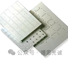
An electronic carrier made of high-purity ceramic material combined with metal thin sheets, possessing both the insulation and heat-dissipation advantages of ceramics and the conductive properties of metal. In essence, it is a combination of a "ceramic base + metal circuitry" that solves the challenge where traditional substrates could not simultaneously achieve insulation and heat dissipation.
02 Development History and Current Status
Three Major Development Stages
1. Beginning (1970s-1990s): Dominated by alumina substrates, simple processes, with core technologies monopolized by Japan and the US, and almost no domestic presence.
2. Growth (2000-2015): Aluminum nitride / silicon nitride substrates became popular; domestically only basic alumina substrates could be produced, with mid-to-high-end products still relying on imports.
3. Upgrade (2016 to present): AI and automotive semiconductors drive demand for high-end substrates, domestic enterprises accelerate technological breakthroughs, entering a critical period of domestic breakthrough.
Current Industry Status
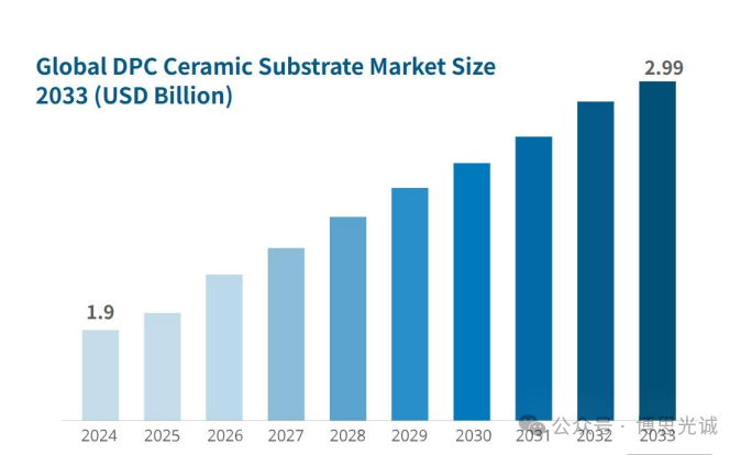
1. Rapid market growth: The global market was about USD 2.8 billion in 2023, expected to reach USD 4.5 billion by 2027 (CAGR≈12.5%); China is one of the largest consumer markets, with the domestic market expected to reach RMB 8 billion in 2025.
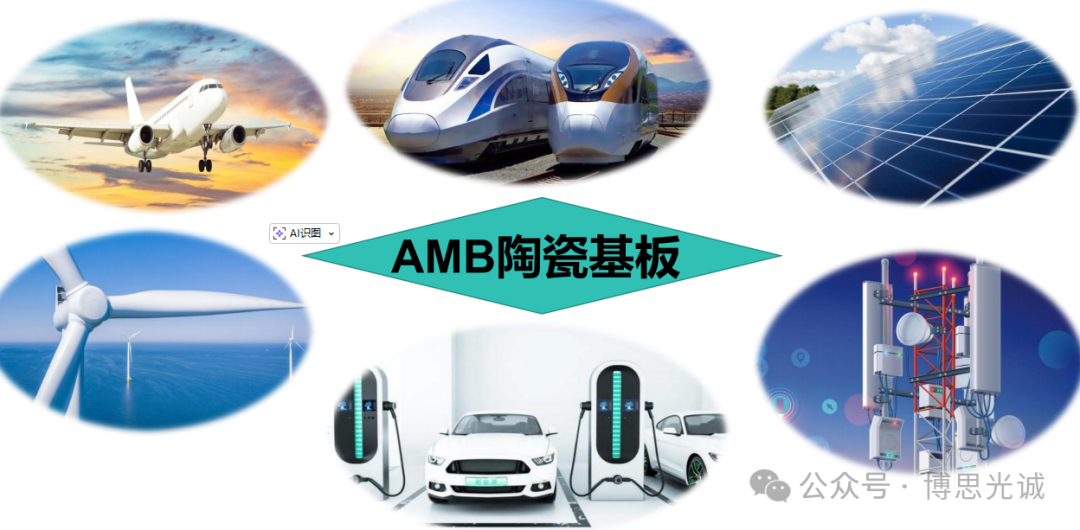
2. Demand structure upgrade: Upgrading to high-end aluminum nitride and silicon nitride substrates, with AMB technology becoming a hot topic; new energy vehicles and AI chips are core drivers.
3. Accelerated domestic substitution: Enterprises such as Jiangfeng Electronics and ZheCi Electronics have broken through core technologies including powder preparation and AMB process; comprehensive substitution achieved in mid-to-low-end products, high-end products passing automotive/military certifications. However, a gap with overseas remains, with enormous substitution potential.
03 Main Classifications
Primarily divided by material and process, with different types suited to different scenarios, forming the industry's mainstream classification dimensions:
By Core Material (4 Mainstream Types in the Market)
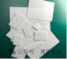
1. Aluminum oxide:
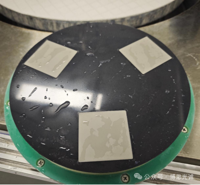
2. Aluminum nitride:
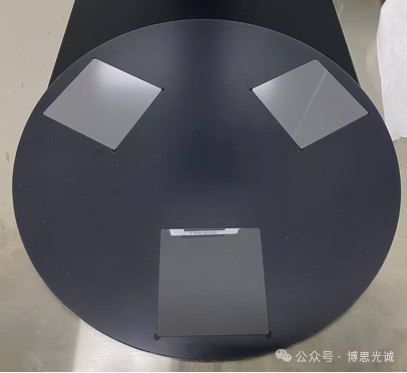
3. Silicon nitride:
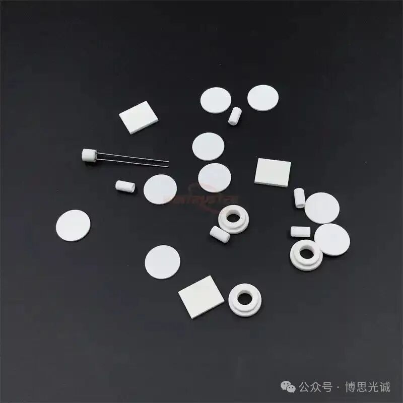
4. Beryllium oxide:
By Manufacturing Process (Industry Hot Topics: DBC, AMB, LTCC)
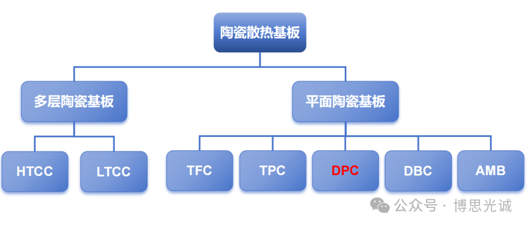
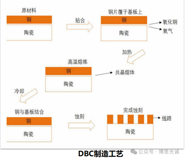
1. DBC (Direct Bonded Copper): The mainstream process for mid-to-high-end high-power equipment, with copper foil and ceramic sheets tightly bonded at high temperature, offering good heat dissipation and suiting new energy vehicle power components.
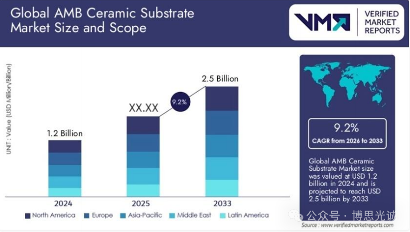
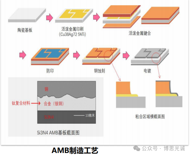
2. AMB (Active Metal Brazing): An upgraded high-end process of DBC with stronger bonding, suited to high-voltage, high-current scenarios; 3-5 sheets are needed per electric vehicle.
3. LTCC (Low-Temperature Co-fired Ceramic): Enables three-dimensional wiring, suited to miniaturized, high-frequency scenarios such as 5G equipment and automotive radar.
4. HTCC (High-Temperature Co-fired Ceramic): An early high-end process with high firing temperatures and high costs, mainly used in aerospace and military applications.
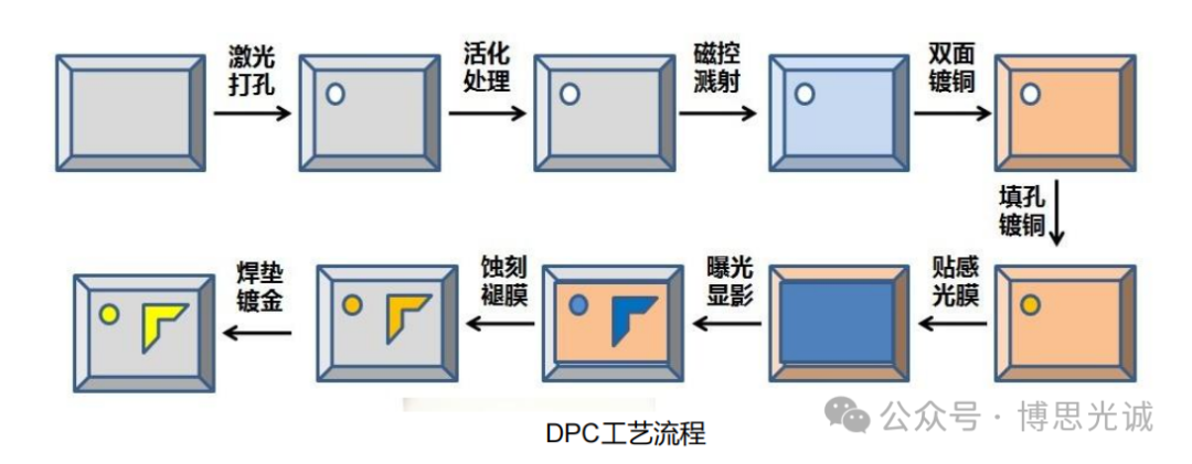
5. DPC (Direct Plated Copper): High circuit precision, accounting for 69% of the ceramic substrate market in the LED field.
04 Four Core Functions
Ceramic substrates are the "four pillars" of semiconductors, with each function indispensable, directly determining device performance and lifespan:
Support and Fixation: Provides a stable platform and precise positioning for chips and components, ensuring complete circuit structure.
Heat Dissipation and Conduction: Rapidly draws out the heat generated by chip operation to avoid lag and damage, one of the most core functions.
Insulation and Isolation: Isolates signal interference between circuits, withstands high voltage, prevents short circuits, and ensures equipment stability.
Electrical Interconnection: Transmits electrical signals and power through metal circuitry; circuit precision is key to equipment miniaturization.
05 Four Key Core Technology Breakthrough Points for Domestic Breakthrough
Domestic technical bottlenecks are concentrated in high-end materials, core processes, and precision control. The breakthroughs focus on four areas:
1. High-end ceramic powder preparation: Improve the purity (over 99.9%) and particle uniformity of high-end powder, reduce costs, and achieve upstream self-reliance.
2. High-end bonding process (AMB): Optimize soldering materials and processes, solve the porosity problem, and improve bonding strength, high-temperature resistance, and impact resistance.
3. Wiring precision improvement: Optimize processes to achieve the high-end requirement of line width ≤20 micrometers, suited to high-density, high-precision scenarios such as AI chips.
4. Cost control and scale-up: Optimize production processes, improve yield, develop low-cost solutions, improve integrated industrial chains, and drive the popularity of high-end substrates.
BOSI Kousei Seimitsu
A Solution Provider Focused on "Cutting," "Grinding," and "Polishing"
Ceramic substrates are the "must-win battleground" of domestic semiconductors, and their technical level is directly related to the self-reliance and controllability of China's semiconductor industry. Currently, comprehensive substitution has been achieved in the domestic mid-to-low-end market, and the high-end market is accelerating breakthroughs. In the future, the industry will develop toward higher thermal conductivity, higher precision, and lower cost, becoming an important support for the domestic semiconductor breakthrough and continuously empowering new industries such as new energy vehicles, AI, and aerospace. Nanjing BOSI Kousei Seimitsu Technology Co., Ltd. is deeply engaged in the precision processing of ceramic substrates. Closely following industry trends and customer needs, and backed by professional technology and full-process service experience, the company can tailor exclusive ceramic substrate lapping and polishing solutions for customers in different scenarios, precisely matching needs, solving processing pain points, helping customers enhance competitiveness, jointly promoting the upgrade of the domestic ceramic substrate industry, and empowering the self-reliance and controllability of the semiconductor industry.


