
Polishing Pad: The "Invisible Flatness Master" of Precision Manufacturing
In high-end manufacturing fields such as semiconductors, optical glass, precision ceramics, and sapphire, there is a core consumable that is low-key yet determines the quality of the finished product—the polishing pad.
It is not merely a "polishing cloth," but rather a key role that commands precision, yield, and efficiency in the Chemical Mechanical Polishing (CMP) process. Today, we will systematically introduce what a polishing pad is, what it does, and how to choose one.
01 Polishing Pad: What Exactly Is It?
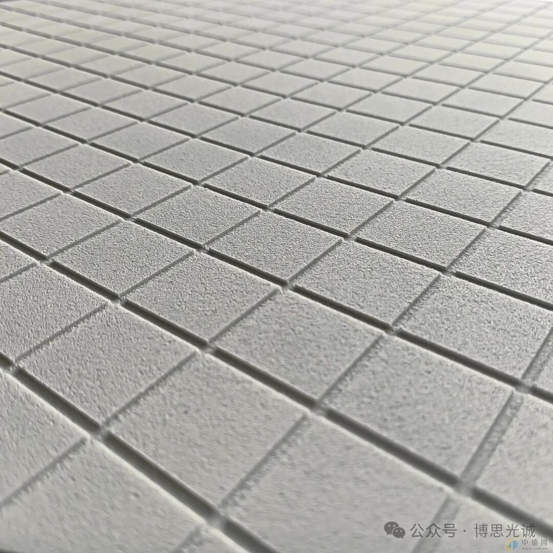
A polishing pad (also called polishing skin or polishing sheet) is a core consumable in precision polishing. Through the synergistic action of "chemistry + mechanics," it polishes the workpiece surface to nanometer-level finish and flatness.
Put simply:
It is the "lapping stage" that carries the polishing slurry, applies uniform pressure, and removes debris while dissipating heat, directly determining whether the final surface is scratch-free, damage-free, and ultra-flat.
02 Core Functions: 4 Irreplaceable Key Roles
Uniform Force Transfer
Stabilizes pressure distribution, avoids local over-polishing/under-polishing, and ensures full-surface consistency.
Slurry Storage and Debris Removal
Micro-pore/groove structures store the polishing slurry and promptly carry away debris, preventing scratches on the workpiece.
Heat Dissipation and Temperature Control
Rapidly conducts away friction heat, avoids high-temperature deformation, and stabilizes the process window.
Precision Definition
Hardness, elasticity, and structure match the process, enabling full control from rough polishing to fine polishing.
03 Mainstream Types and Applicable Scenarios
Polyurethane Polishing Pad (Mainstream for CMP)
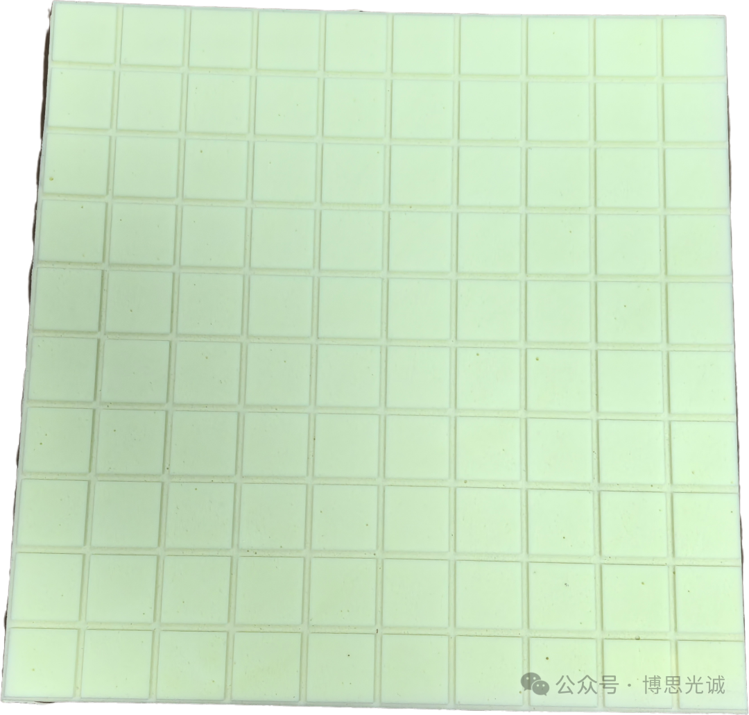
Features: Adjustable hardness, excellent flatness, stable lifespan
Applicable to: High-precision fields such as semiconductor wafers, silicon wafers, silicon carbide, and precision ceramics
Non-Woven Fabric / Backing Pad Polishing Pad
Features: Good elasticity, high porosity, conforms to curved surfaces
Applicable to: Optical glass, lenses, sapphire, and ceramic substrate rough/mid polishing
Composite / Special Polishing Pad
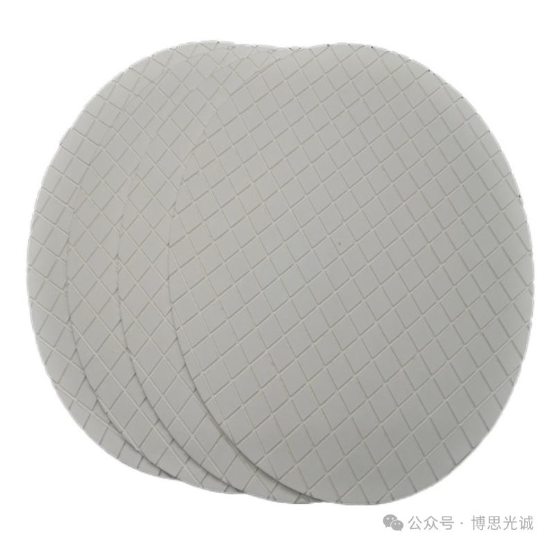
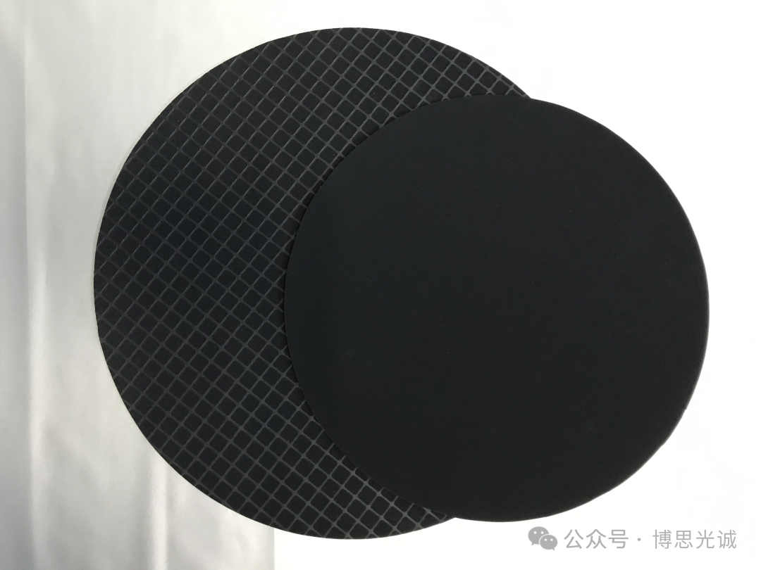
Features: Adjustable hardness, excellent flatness, stable lifespan
Applicable to: High-precision fields such as semiconductor wafers, silicon wafers, silicon carbide, and precision ceramics
04 Why Is Choosing the Right Polishing Pad Important?
Directly improves yield and reduces scrap and rework
Stabilizes nanometer-level flatness and meets high-end process requirements
Extends service life and lowers per-unit consumption costs
Matches the polishing slurry to maximize the efficiency of the entire process
In high-precision industries such as chip manufacturing, optoelectronics, and precision ceramics, one grade lower in the polishing pad means one grade lower in the finished product.
05 Selection: Focus on These 3 Points to Avoid Detours
Look at Material Hardness
Hard pad → high removal rate; soft pad → low damage, high finish.
Stabilizes nanometer-level flatness and meets high-end process requirements
Flat/mesh/spiral/micro-pore, matching debris removal and flatness needs.
Directly improves yield and reduces scrap and rework
Rough polishing emphasizes efficiency, fine polishing emphasizes finish, and final polishing emphasizes zero damage.
END
Though small, the polishing pad is the flatness cornerstone of precision manufacturing. From chips to lenses, from sapphire to ceramic substrates, it supports nanometer-level precision with its micron-level structure. Good polishing starts with choosing the right polishing pad.
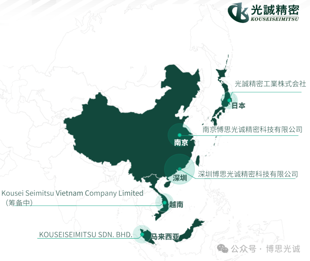
Kousei Seimitsu is a globally positioned comprehensive enterprise in the lapping and polishing field, dedicated to providing customized lapping and polishing solutions for high-end manufacturing sectors such as precision optics, semiconductors, and precision ceramics.
Backed by a standardized testing system, the company conducts multi-dimensional field-test verification for different workpiece needs, precisely matching lapping consumables and process parameters. With professional technical strength and strict quality control, Kousei Seimitsu can tailor efficient and precise processing solutions to customers' personalized needs, helping customers overcome various polishing challenges and earning broad market recognition.


