
The Chip Tide Rises, Drawing a Blueprint Together | SEMICON China 2026 Exhibition Review
On March 25-27, SEMICON China 2026, the annual grand event of the global semiconductor industry, concluded successfully at the Shanghai New International Expo Center. Under the theme "Crossover Global, Connecting Minds & Chips," this exhibition brought together 1,500 global exhibitors and 5,000+ booths, attracting 180,000+ professional visitors. It comprehensively covered the entire pan-semiconductor industry chain—chip design, manufacturing, packaging and testing (OSAT), equipment, and materials—becoming a core platform for insight into industry trends, connecting global resources, and driving technological innovation.
01 Exhibition Highlights: Full-Chain Assembly, Overwhelming Popularity
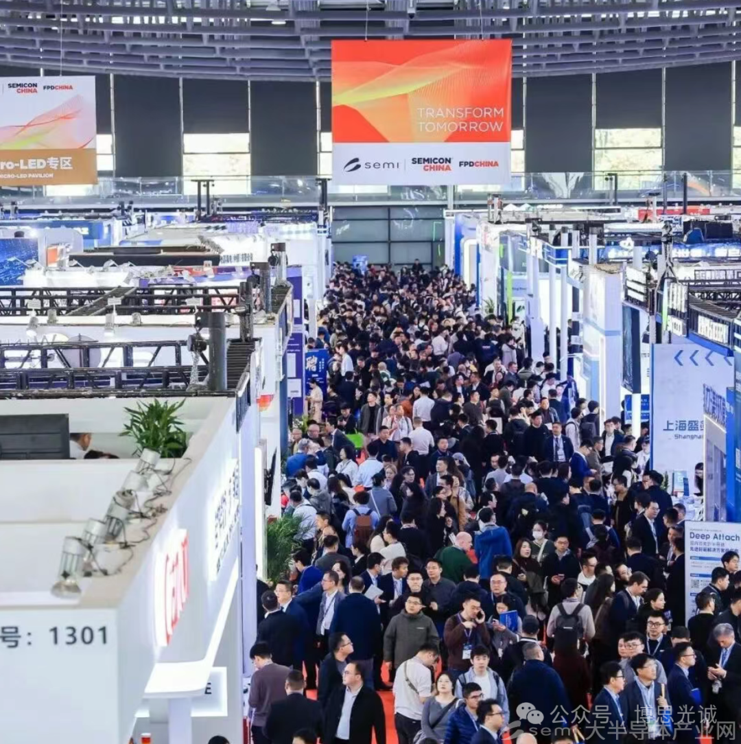
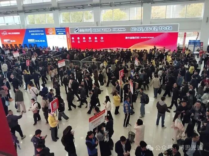
Scale and specifications reached new heights. The exhibition area exceeded 100,000 square meters, covering multiple halls including N1-N5 and E6-E7, with both exhibitor and professional visitor numbers hitting new highs in recent years. From international giants to local rising stars, from equipment and materials to design and packaging and testing, enterprises across the entire industry chain appeared on the same stage. The venue was bustling with people and enthusiastic negotiations, fully demonstrating the vibrant vitality of the semiconductor industry.
Rich Concurrent Events
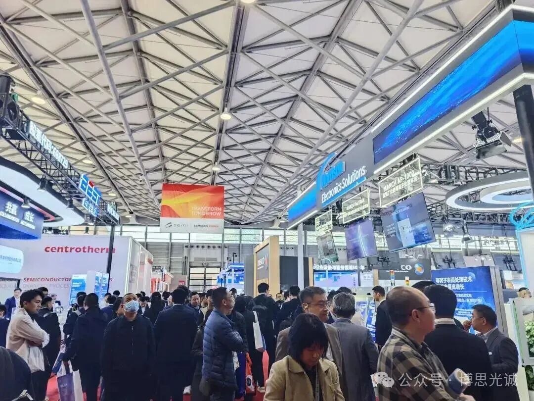
Concurrently, the exhibition hosted 20+ high-end forums and technology summits, including authoritative conferences such as the China Semiconductor Technology International Conference (CSTIC) and the China Display Conference (CDC). Focusing on hot topics such as advanced processes, third-generation semiconductors, AI chips, advanced packaging, and domestic substitution, they brought together global industry leaders, technical experts, and corporate executives to discuss industry development directions and share cutting-edge technical achievements, providing deep intellectual exchange and trend guidance for the industry.
02 Focusing on Core Needs: Customized Solutions Demonstrate Strong Technical Strength
In semiconductor manufacturing, Chemical Mechanical Planarization (CMP) is the key enabling technology for achieving ultra-smooth, defect-free global planarization of wafer surfaces, and the performance of consumables such as polishing pads directly determines the planarization effect, processing efficiency, and product yield. During the exhibition, BOSI Kousei Seimitsu highlighted multiple customized lapping and polishing solutions tailored to different process nodes and customers' actual application needs. Centered on core performance indicators such as high removal rate, excellent planarization capability, and defect control optimization, the company provided customers with full-process, targeted product and process support.
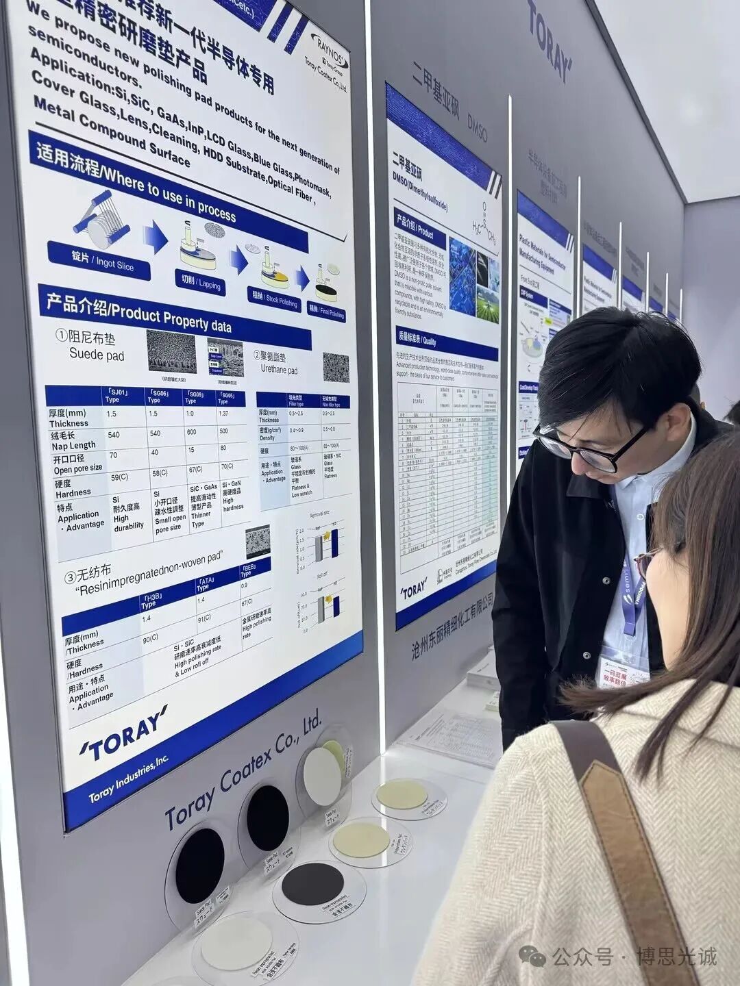
Addressing pain points customers face in actual production—such as insufficient polishing stability, short consumable lifespan, and difficulty controlling surface defects—the BOSI Kousei Seimitsu technical team engaged in deep on-site communication with customers, carefully analyzing their process environments and parameter conditions. They proposed a series of directly actionable improvement suggestions in the structural design of polishing pads, groove design solutions, and lifespan enhancement, helping customers achieve a better balance between processing stability and production efficiency, truly solving production pain points and reducing operating costs.
03 Deep Cultivation of Segmented Scenarios: Multi-Field Breakthroughs Unlock New Application Boundaries
As the semiconductor industry rapidly iterates toward advanced packaging and compound semiconductors, the planarization process faces higher technical requirements. BOSI Kousei Seimitsu focused on two core segmented scenarios, demonstrating strong technical adaptability and innovation capability.
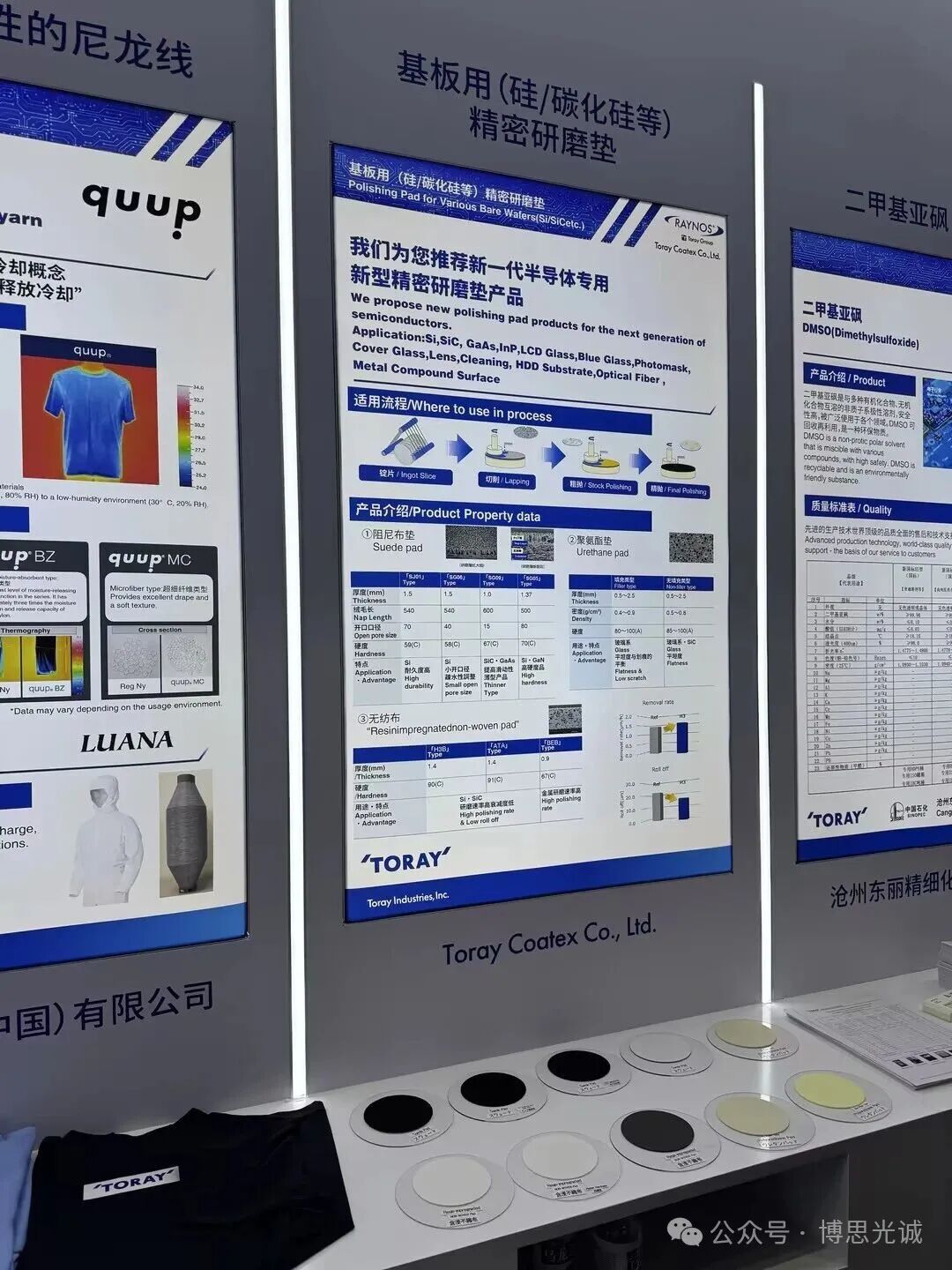
In advanced packaging and TGV glass substrate related applications, glass substrates have become the core solution to break through the performance bottleneck of traditional organic substrates, thanks to their excellent dimensional stability and low dielectric loss, and their surface planarization is key to determining the quality of subsequent packaging. BOSI Kousei Seimitsu focuses on material compatibility and surface quality control. By optimizing the polishing pad structure and interface characteristics, it effectively improves uniformity and consistency during processing, controlling surface roughness and defect rate within strict standards, significantly reducing surface defect risk, helping TGV glass substrates achieve higher-precision processing needs, and adapting to the high-density, high-performance development trend of advanced packaging.
In compound semiconductor material applications, hard-brittle materials such as monocrystalline diamond, silicon carbide, and gallium nitride have become an industry technical bottleneck for planarization processing due to their extremely high hardness and strong chemical inertness. Targeting the characteristics of these materials—high processing difficulty and narrow process windows—BOSI Kousei Seimitsu further expanded the applicable range of polishing pads across different processing processes through multi-dimensional parameter matching and optimization of polishing pad basic performance. It excels in polishing stability and service life, effectively solving the industry pain points of low processing efficiency and easy damage of hard-brittle materials, providing strong support for the large-scale development of the compound semiconductor industry.
04 Collaboration with Partners: Ecosystem Linkage Builds New Industrial Advantages Together
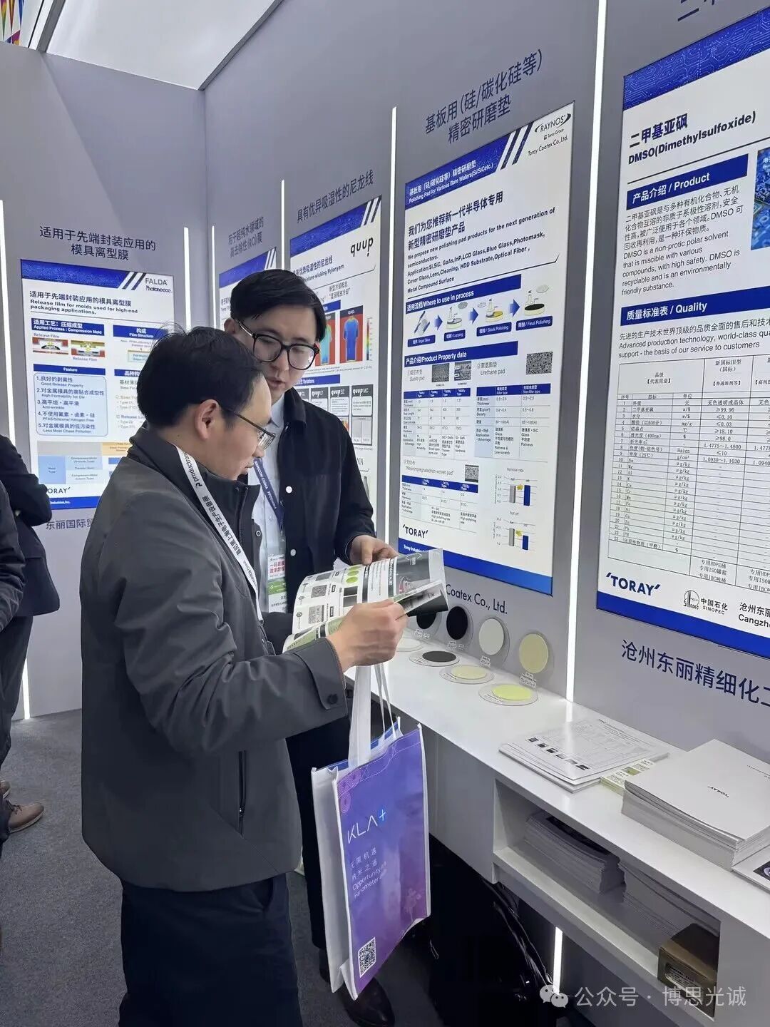
High-quality industrial development cannot be separated from upstream-downstream coordination and linkage. BOSI Kousei Seimitsu always values deep collaboration with partners. Exhibiting together with Toray this time is a vivid demonstration of mutual resource complementation and technological linkage. Leveraging its long-term collaborative relationship with upstream material partners such as Toray, BOSI Kousei Seimitsu continuously introduces advanced material systems and cutting-edge process experience in product R&D and technical support, constantly optimizing product performance and improving solutions, achieving a "1+1>2" cooperative effect.
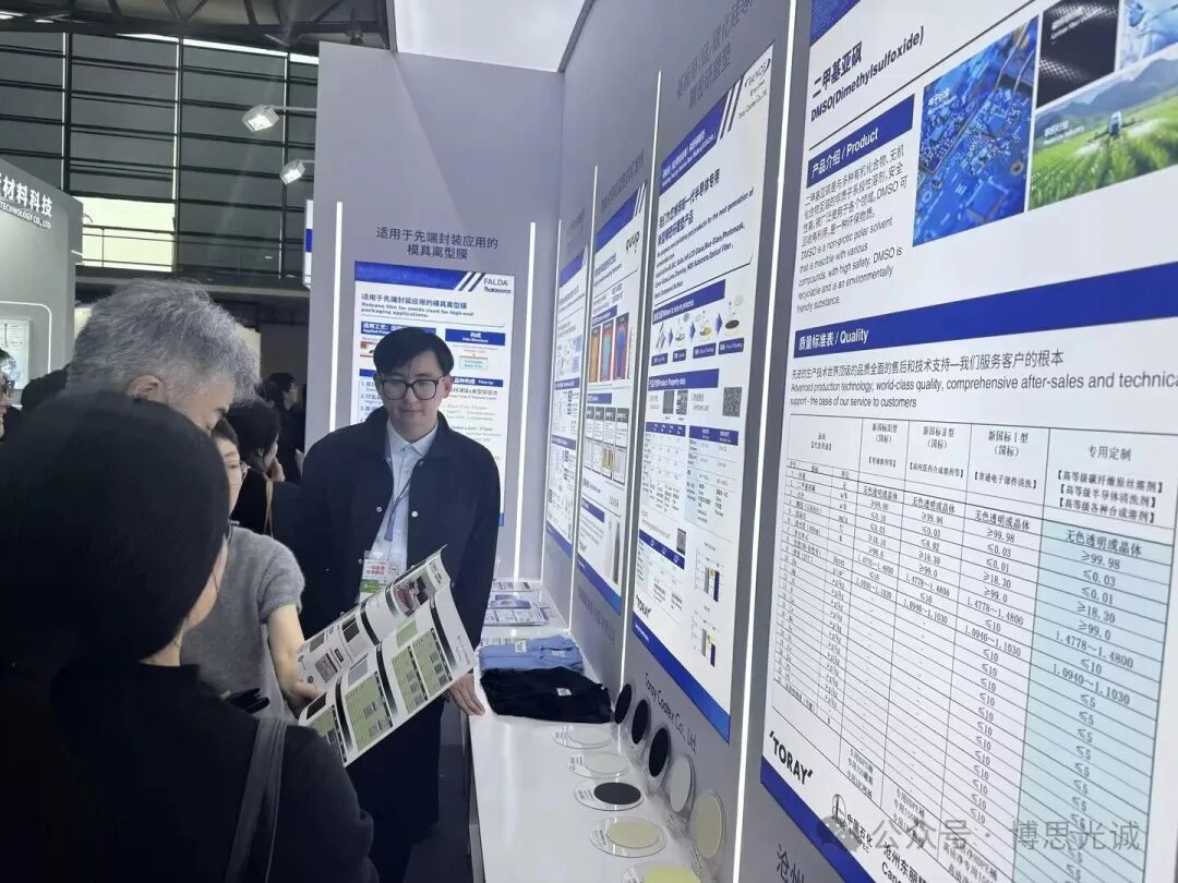
At the exhibition site, through face-to-face technical communication and sharing of typical cases, BOSI Kousei Seimitsu not only provided customers with directly referenceable process paths, but also assisted customers in improving yield performance and reducing overall costs at the practical application level, driving continuous optimization and upgrading of the entire process. Many customers gave high recognition to the company's customized solutions and professional technical services, and multiple cooperation intentions were reached on site, laying a solid foundation for subsequent business expansion.
END
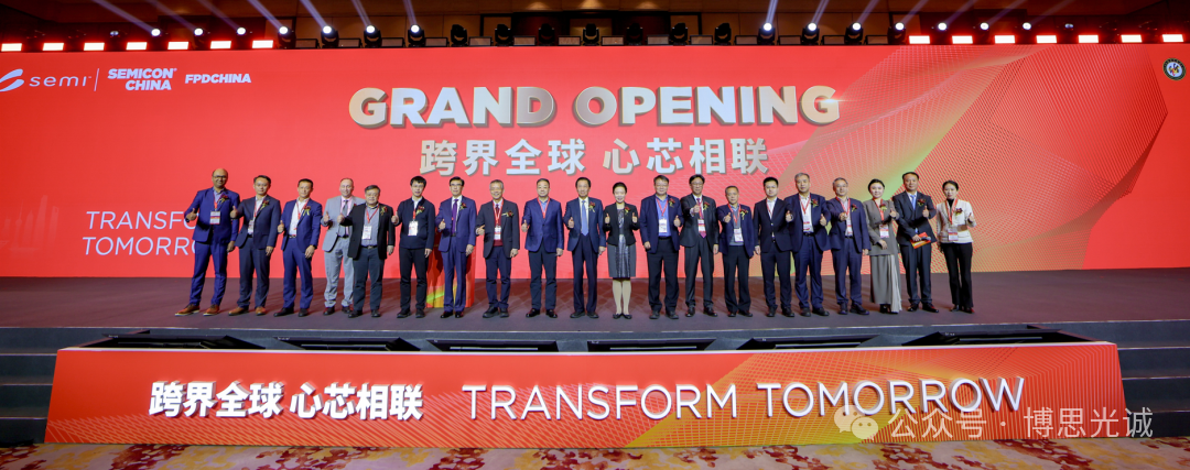
The conclusion of SEMICON China is both an ending and a new beginning. This exhibition not only allowed BOSI Kousei Seimitsu to further showcase its technical strength and brand influence in the semiconductor planarization process field, but also provided deeper insight into industry development trends and core customer needs, and deepened the collaborative consensus with partners.
In the future, BOSI Kousei Seimitsu will continue to uphold its original intent of innovation, deepen collaboration with partners such as Toray, focus on customers' actual needs in different application scenarios, continuously improve its product system and technical service capabilities, deeply cultivate the semiconductor material planarization process field, and commit to providing customers with more efficient, stable, and sustainable integrated cutting, grinding, and polishing solutions, empowering China's semiconductor industry toward self-reliance, controllability, and high-quality development, and drawing a new blueprint for the semiconductor industry together with industry partners.


