
Optical Chip Materials: Exploring InP & GaAs Lapping and Polishing Technology
From Material Challenges to Process Breakthroughs: Exploring the Lapping and Polishing Technology of Indium Phosphide (InP) and Gallium Arsenide (GaAs)
01 The Optical Chip Era: Material Processing Is Facing New Challenges
With the rapid development of 5G communications, high-speed data center interconnects, AI computing networks, and advanced optoelectronic devices, optical communications and optoelectronic integration are becoming important directions for the semiconductor industry. In this process, the importance of compound semiconductor materials such as Indium Phosphide (InP) and Gallium Arsenide (GaAs) continues to rise.
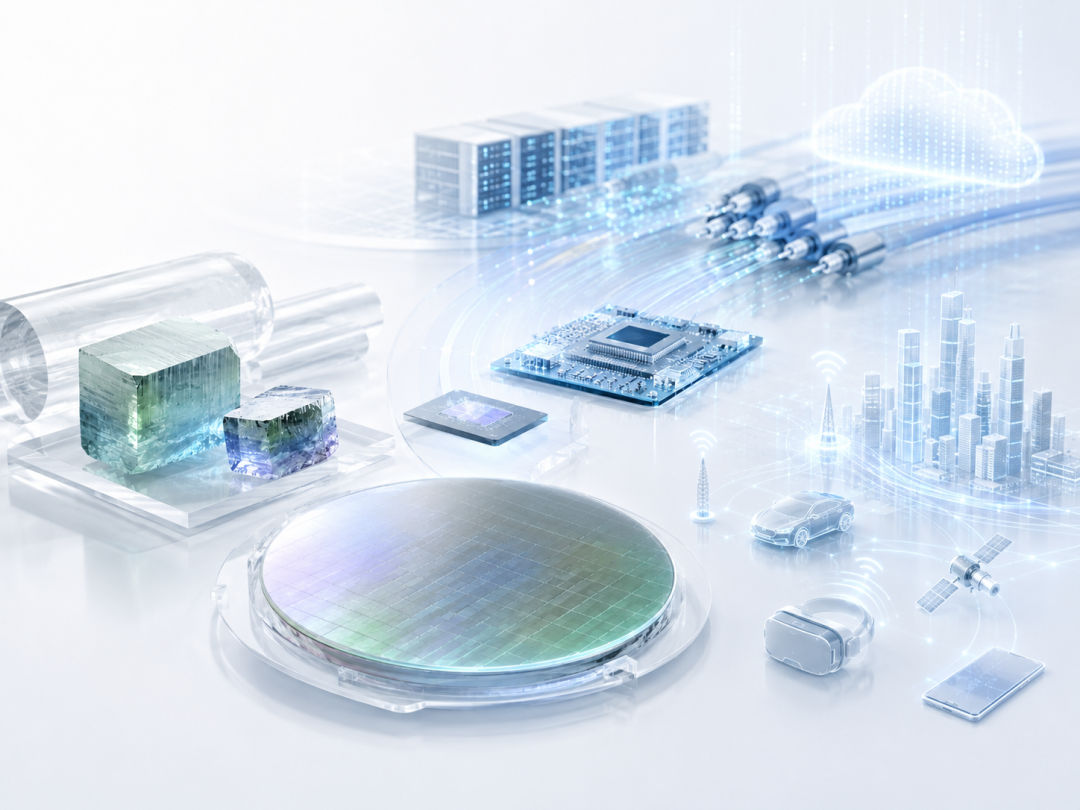
As important representatives of the second-generation III-V compound semiconductors, InP and GaAs possess excellent optoelectronic conversion capability, high-frequency characteristics, and direct bandgap advantages, and are widely used in fields such as high-speed optical communication devices, high-frequency millimeter-wave devices, optoelectronic integrated circuits, and space solar cells.
Concept diagram of compound semiconductor material applications:
However, from monocrystalline material to high-quality wafers meeting device manufacturing requirements is not a simple cutting and shaping process. The lapping and polishing processes directly determine the wafer surface flatness, defect control capability, and subsequent epitaxy quality, making them important stages affecting device performance and yield.
02 InP and GaAs: Both Compound Semiconductors, yet with Different Processing Difficulty
Gallium Arsenide (GaAs) has good mechanical stability, and its related processing processes are currently relatively mature, with substantial application experience in wafer manufacturing, optoelectronic devices, and high-frequency devices.
In contrast, Indium Phosphide (InP) has a "soft and brittle" material characteristic, making it more prone to surface damage layers, subsurface cracks, edge chipping, and wafer warping during lapping. This means that InP processing must not only focus on removal efficiency, but also on controlling processing stress and surface defects.
Research data shows that under the same mechanical lapping conditions, the deformed layer thickness generated by InP is about 2.5 times that of GaAs. Therefore, the lapping and polishing process window for InP is narrower, placing higher demands on polishing slurry, polishing pad, pressure, speed, and processing stability.
03 Removal Efficiency and Surface Quality: The Core Challenges of InP Processing
Under the same process conditions, the rough polishing removal rate of GaAs is about 0.7-1.0μm/min, while that of InP is about 0.10-0.15μm/min. Compared with GaAs, the material removal efficiency of InP is notably lower, which directly affects processing pace and mass production efficiency.
For optoelectronic device manufacturing, wafer surface roughness generally needs to be controlled at the nanometer level. If the surface has scratches, pits, residual damage layers, or subsurface cracks, it may affect subsequent epitaxial growth quality and further affect device performance and reliability.
Therefore, the difficulty of InP processing is not just "grinding fast," but improving removal efficiency while minimizing mechanical damage to achieve stable, repeatable, and mass-producible surface processing results.
04 CMP Technology Drives the Upgrade of Compound Semiconductor Processing
Chemical Mechanical Polishing (CMP) is a precision processing technology combining chemical reactions and mechanical removal. Its basic principle is to form an easily removable reaction layer on the material surface through chemical action, then combine it with abrasives and a polishing pad for precise removal, thereby obtaining a wafer surface with high flatness and low damage.
For compound semiconductor materials such as InP and GaAs, CMP is not only related to surface roughness control, but also to surface defects, processing damage layers, and subsequent process compatibility. Compared with pure mechanical lapping, CMP is more suitable for high-quality wafer surface processing.
However, traditional InP polishing systems still have problems such as volatility, safety, particle adhesion, and insufficient stability. Therefore, developing polishing slurry systems and process combinations better suited to InP material characteristics is the key direction for improving processing quality and mass production stability.
05 Kousei Seimitsu's Self-Developed Series: Optimized Solutions for InP Processing Needs
Addressing the problems of traditional InP polishing systems, our company has developed the KSTP-801~804 series alumina polishing slurries. This series of products is designed for the rough polishing process of compound semiconductor materials such as InP, with a focus on optimizing material removal efficiency, surface quality, and process stability.
KSTP-801~804 series alumina polishing slurry product image:
While ensuring surface processing results, the KSTP-801~804 series can achieve a maximum removal rate of 2.5um/min, helping to improve the problem of low InP processing efficiency and providing a more stable foundation for subsequent fine polishing and surface optimization processes.
Product features include:
1. Designed for the soft-brittle characteristics of InP material;
2. Optimized processing efficiency in the rough polishing stage;
3. Reduced risk of surface damage and scratches;
4. Improved polishing process stability and process repeatability.
In addition to the KSTP-801~804 series rough polishing solutions, our company has also developed the KSTP-SP20 silica polishing slurry for the InP substrate fine polishing process.
This product adopts a two-component silica system, suitable for fine polishing processing of InP chip substrates, with a focus on low roughness, low damage, and high surface quality requirements. Through process matching with consumables such as the KS09 polishing pad, the surface convergence effect in the fine polishing stage can be further improved.
KSTP-SP20 silica polishing slurry product image:
In related process verification, KSTP-SP20 can converge the surface roughness of InP substrates after fine polishing to Ra < 0.2nm, providing stable support for subsequent chip processes and high-quality surface requirements.
Product features include:
1. Designed for the InP substrate fine polishing process;
2. Adopts a two-component silica polishing system;
3. Helps reduce surface roughness;
4. Final surface roughness can be converged to Ra < 0.2nm;
5. Can form a stable process match with the KS09 polishing pad.
Addressing the requirements for surface quality and processing efficiency during InP chip backside polishing, our company has developed the KSTP-IP80 polishing slurry.
This product is mainly used in the InP chip backside polishing process, with a focus on high flatness, low roughness, and stable removal effect requirements. Through reasonable polishing slurry system design and polishing pad matching, KSTP-IP80 can achieve relatively stable processing efficiency while ensuring surface quality.
KSTP-IP80 alumina polishing slurry product image:
In related process verification, after backside polishing with KSTP-IP80, the surface roughness can reach Ra < 0.2nm and the removal rate can reach 2μm/min, suitable for InP chip backside polishing scenarios with high surface quality requirements.
Product features include:
1. Designed for the InP chip backside polishing process;
2. Surface roughness can reach Ra < 0.2nm;
3. Removal rate can reach 2μm/min;
4. Balances processing efficiency and surface quality, suitable for high-precision chip backside polishing needs;
For sample testing, please contact Engineer Wang at 13312961176 (same as WeChat).
06 Polishing Pad: The Key Consumable Determining CMP Stability
In the CMP process, the polishing pad not only supports the wafer and transmits pressure, but also affects polishing slurry distribution, debris removal, material removal uniformity, and surface defect control.
For soft-brittle materials such as InP, the choice of polishing pad is particularly critical. If the polishing pad is too hard, it may increase the risk of surface scratches and subsurface damage; if support is insufficient, it may affect flatness and removal uniformity.
Therefore, the polishing pad needs to strike a balance between reducing mechanical damage and ensuring removal efficiency, and must be matched synergistically with parameters such as the polishing slurry system, processing pressure, and speed to achieve stable CMP processing results.
07 KS09 Backing Pad: Achieving High-Quality Processing Matching
In actual process verification, our company used the KS09 backing pad polishing pad, represented from Japan's TORAY, together with the KSTP-IP80 series polishing slurry for InP fine polishing processing.
KS09 backing pad polishing pad product image:
This combination can effectively control wafer surface defects during fine polishing and reduce the risk of scratches during processing. Through the synergistic matching of polishing slurry and polishing pad, the InP wafer surface quality and processing stability can be further improved.
Actual verification results show that this combination can achieve scratch-free results under strong light in the fine polishing stage, providing a more reliable surface foundation for subsequent cleaning, inspection, and device manufacturing processes. For sample testing, please contact: Engineer Wang at 13312961176 (same as WeChat).
08 Conclusion
With the continuous development of high-speed optical communications, AI computing networks, data center interconnects, and advanced optoelectronic devices, compound semiconductor materials such as InP and GaAs will play an even more important role in the future industry.
At the same time, high-quality wafer processing capability will become an important foundation supporting the application of materials. The lapping and polishing processes not only affect wafer surface quality, but also relate to subsequent epitaxy, device manufacturing, and final product reliability.
BOSI Kousei Seimitsu will continue to explore new polishing slurry systems, multi-step polishing processes, and dedicated polishing pad matching solutions. Through the synergistic optimization of materials, consumables, and processes, we will provide high-performance lapping and polishing solutions for the semiconductor and advanced manufacturing fields.
About Us
BOSI Kousei Seimitsu was founded in July 2022, focusing on integrated cutting, grinding, and polishing solutions in the precision processing field. It is an enterprise integrating equipment agency, consumable R&D, process customization, and import/export services. The company focuses on the semiconductor, precision optics, and special ceramics industries, providing stable and reliable one-stop services for high-end manufacturing through high-precision lapping, polishing, and cutting products and technical support, helping customers improve quality and efficiency.
Positioning: Full-process equipment and consumable provision and process solution development for the lapping and polishing industry.
Company business: Precision processing consumables and equipment, self-developed product R&D, and technical solution services.
Main business:
① Supply of production consumables such as thinning wheels, lapping and polishing slurries, polishing pads, and ceramic balls.
② Improvement of existing process solutions and R&D of new solutions in the lapping and polishing industry.
Deep-cooperation partners: internationally renowned enterprises such as NORITAKE, TORAY, and Sumitomo Chemical.


